[ad_1]

Here is a simple FM Radio Receiver Using single chip TA 2003. This IC have inbuilt RF Amplifier, local oscillator, a mixer, FM detector and AF preamplifier. Only few passive components like ceramic capacitors, X1, X2 both are 10.7MHz 3-pin, 2-pin, homemade inductors like L1, L2 and L3,an electrolytic capacitor 2.2uF/25V are used in this circuit. 10.7 MHz IFT coil is not used here so there is no need to tune of coils.

Parts List
| Semiconductors IC1: TA 2003 Ceramic capacitors Electrolytic Capacitor Ceramic Filter Miscellaneous |
Circuit Description
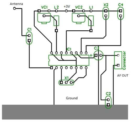
Pin 1 of IC1 TA 2003 is connected to antenna (75cm long wire) through C1. A capacitor C3 is c. Pin 2, pin 9 are grounded.
A crystal 10.7 MHz 3-pin is connected to pin 3 and 8 (colour tag is faced towards pin 3) and middle pin is connected to+3 Vcc.
Pin 13 is connected to coil L2 and VC1b in parallel to each other . Other one end is connected to +3 Vcc. Pin 6 and pin 14 are connected to +3Volts. A coil L1 and VC1b are connected to each other in parallel. One end of L1 and VC1a is connected to pin 15 and others end is connected to +3Vcc. Pin2, 9 are grounded.
Ceramic filter X2 (10.7 MHz 2-pin) is connected to +3 Vcc and pin 10. Pin 11 is an output pin and is connected to AF amplifier through an electrolytic capacitor 10uF/25V. A capacitor C4 is an electrolytic capacitor is of (220uF/25V) connected to negative terminal and +3Vcc which will filter a DC +3Vcc.voltage. And capacitor C2 will filters a noise represent at AF output. And an AF output is taken output from pin 11 of IC1 through an electrolytic capacitor C3 (10uF/25V).

Construction
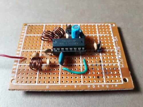
A veroboard of 5cmX7cm is suitable to build your prototype. A PCB layout is given in the article is suitable to build your prototype.
Now you’ll make coil L1, L2. For a coil L1 a 22SWG wire is wound on 5mm diameter with 3 turn’s air core and coil L2 is 22 SWG wire 5mm diameter wound on 4 turns of air core.
Now insert an 16-pins IC socket on a middle of a vero board and solder it. Now take an IC1 TA 2003 and place it on an 8-pin IC socket. Next insert a coil L1, L2 as given in a diagram and also X1(3-pins 10.7MHz ceramic filter), and X2 (2-pin 10.7MHz ceramic filter). You may place 2-pin connector for AF output and also for +3 V and negative terminal of+3V battery.

Calibration and Adjustment
For a calibration you need an AF amplifier which is connected to output pin 11 of IC1. Take a 2*1.5 Volts battery and connect both 1*2 V battery in series and connect to a +3V terminal and ground)
Now turn a volume of AF amplifier. You will hear a snowy as on TV set. Next gently adjust coil L1and L2 by pulling them apart You may catch some of FM stations. Connect VC1a and VC2b gang variable capacitor in parallel with L1, L2. Tune a VC1a, b to a most powerful station. As soon as you will hear a clear and loud sound, you may tune to different stations.
Source link

